Glass Material Supply and Precision Fabrication for Semiconductor and Optical Applications
By combining carefully selected glass materials from leading manufacturers in Japan, Korea, Germany, China, and other countries with our patented high-precision processing technology, We ensure exceptional cleanliness, superior surface accuracy, high transmittance, excellent homogeneity, and reliable supply.
Who We Are
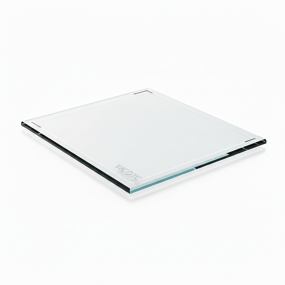
We are shaping new value through high-quality glass material supply from Japan, Germany, Korea, and China, combined with custom high-precision processing for Semiconductor and Optical applications.
Business overview

Glass Materials
for Semiconductor Applications
Photomask Substrates
Applicable Materials: Fused Silica & Synthetic Quartz
-
Material Purity & Internal Defects
-
Flatness, Parallelism & Thickness Uniformity
-
Ultra-Low Surface Roughness & Minimal Subsurface Damage
-
Low Particle Contamination, Low Impurity Levels & Low Defect Density
-
Refractive Index Uniformity, Low Birefringence & Thermal Stability
-
Production Consistency & Traceability

Glass Materials
for Optical Applications
Optical Windows
Widely Used in Biomedical, Optoelectronic Communications, Optical Equipment, and Laser Components
-
Material Purity & Internal Defects
-
Surface Figure Accuracy, Parallelism & Wedge Angle
-
Surface Roughness & Subsurface Damage
-
Particle Control, Contamination & Surface Defect Density
-
Transmittance, Birefringence & Thermal Stability
-
Production Consistency & Traceability
-
Coated Windows: Coating Adhesion, Coating Uniformity, Spectral Transmittance & Reflectance
-
Laser Windows: Laser Damage Threshold, Absorption Rate
-
High-Precision Imaging: Wavefront Distortion, Scattering & Haze
-
Space / Outdoor / Harsh Environments: Environmental Resistance, Thermal Shock Stability

High-Precision Custom Machining
Ultra-Thin (150μm and above)
Super-Thin (300 μm to 700 μm and above)
-
Photomask Substrates
Low slicing stress, crack-free, no edge chipping, full-area and local thickness uniformity, parallelism, initial flatness, reduced downstream polishing removal, and low TTV -
Optical Windows
Surface figure optimization, wedge angle control, coating processes, spectral / wavefront inspection -
Reliability Validation
Low internal defects, bubbles, and striae; cutting orientation matched to material characteristics -
Dimensional Precision
Outer diameter / length and width accuracy, thickness accuracy, edge chamfering, concentricity or profile tolerances

Technical Advantages
By integrating the rigorous manufacturing disciplines and advanced technologies of Japan, Germany, Korea, and China in semiconductor photomask and optical glass processing, we consistently deliver high-quality semiconductor glass materials and customized machining services to customers across Europe, the United States, and Japan—helping maximize the performance of your products.
We’d love to hear from you
LINE ID : WCOTCWY
Add us on LINE for immediate contact !!
https://line.me/ti/p/k9DI35XlqA
You can also reach us by email
-
Purchasing & Inquiries: Service@wcotc.com
-
Business Inquiries: Info@wcotc.com
